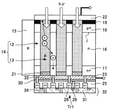
Sony hybrid organic & inorganic sensor patent, the patent describes the sensor is made up of both organic and inorganic materials, the major details below
Translated by google
Sony patents pending on the imaging element of the hybrid formula that combines the benefits of both organic and inorganic materials. Also excellent resolution, there is no false colors since it does not require further OLPF In addition, the high sensitivity superior to be done by the organic photoelectric conversion layer. The organic layer is not suitable as high-speed readout, inorganic layer is done in the movement of the charge, seems to have and also allows high-speed readout. It might have appeared to great imaging element in the future.
Self-interpretation and summary, Patent Document
- Patent Publication No. 2012-49289
- 2012.3.8 Release Date
- 2010.8.26 filing date
- Known art
- Silicon photodiode based on the (hereinafter, PD)
- A typical imaging device of this type
- (Causing a false color) low-pass filter must have a color filter or
- Electron transfer rate is faster
- Drive can be stable at high speed
- Light absorption rate is poor
- Also need 3μm thickness of the PD
- A certain amount of light loss due to a color filter or low-pass filter
- Organic layer
- Using the organic film with a sensitivity to each wavelength
- Low-pass filter and a color filter (false color does not occur) unnecessary
- For light absorption coefficient is greater than the silicon, thin film can be
- You can create a variety of shapes
- Mobility of electrons is small
- Non-high-speed operation
- With current technology, adhesion, durability, there is a difficulty in mass production
- Silicon photodiode based on the (hereinafter, PD)
- Sony’s patent
- Organic layer
- Photoelectric conversion is performed
- The shape of the cylinder
- RGB three types of organic material are stacked in the depth direction
- Inorganic layer (semiconductor layer)
- Charge transfer is carried out
- Leads to a charge storage section
- Back-illuminated (BSI)
- Organic layer
Read more egami (japanese blog)


