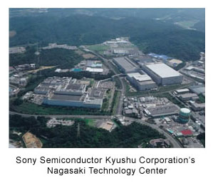
Sony is ready invest approximately 100 billion yen in Sony Semiconductor Kyushu Corporation’s Nagasaki Technology Center, These investments will further strengthen Sony’s production capacity for “Exmor” and “Exmor R” CMOS image sensors in order to meet increased demand from markets such as those for smartphones and Digital Still Cameras.
Press Release
— investment of approximately 100 billion yen in contemplated acquisition of fabrication facilities and expansion of production lines —
— Utilizing a governmental subsidy of the Ministry of Economy, Trade and Industry in Japan —
December 24, 2010, Tokyo, Japan – Sony Corporation (“Sony”) today announced that Sony plans to invest approximately 100 billion yen in Sony Semiconductor Kyushu Corporation’s Nagasaki Technology Center (“Nagasaki TEC”) in the fiscal year ending March 31, 2012, to increase the production capacity for CMOS image sensors.
This investment plan includes (i) the transfer of the semiconductor fabrication facilities from Toshiba Corporation (“Toshiba”) contemplated under a non-binding memorandum of understanding between Sony and Toshiba jointly announced on December 24, 2010, (ii) refurbishment of a part of the above semiconductor fabrication facilities into new wafer lines capable of manufacturing CMOS image sensors, and (iii) refurbishment and equipment of a part of production facilities at Nagasaki TEC Building 3 for wafer processing to differentiate Sony’s CMOS image sensors with Sony’s independently developed unique technologies.*1 Through the investment plan, Sony will utilize a governmental subsidy to be provided by the Ministry of Economy, Trade and Industry in Japan – the “subsidy for programs to promote siting low-carbon job-creating industries” – mainly in connection with the investment mentioned in (iii) above.
These investments will further strengthen Sony’s production capacity for “Exmor” and “Exmor R” CMOS image sensors in order to meet increased demand from markets such as those for smartphones and Digital Still Cameras. Through this increase of capacity, Sony expects to solidify its position as the world’s leading company in CMOS image sensors and CCD image sensors.
As a result of the investments announced today, in addition to the approximately 40 billion yen investment in Sony Semiconductor Kyushu Corporation’s Kumamoto Technology Center (announced on September 1, 2010), Sony’s total production capacity for CCD and CMOS image sensors will increase from the current level of approximately 25,000 wafers per month to approximately 50,000 wafers per month by the end of March 2012.*2


